NVIDIA’s H100/H200, B100/B200, B200/GB200, and HGX/DGX series are high-performance computing platforms designed for different computing needs and are widely used in artificial intelligence (AI), deep learning, big data analysis, scientific computing, and other fields. This article will focus on their differences and parameters.
Оглавление
ToggleChanges to the Nvidia H200 and H100
The NVIDIA H100 and H200 series are primarily high-performance computing platforms based on the NVIDIA Hopper architecture. The H100 uses the latest Hopper architecture, which is deeply optimized for AI and HPC tasks.
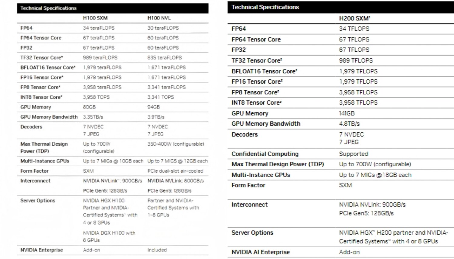
As an upgraded product of H100, H200 actually only upgrades the GPU memory related content in terms of overall parameters, and the GPU single card is upgraded from 80G HBM3 to 141G HBM3e (the memory capacity and type have changed), and the memory bandwidth has been increased from 3.35TB/s to 4.8TB/s, and the overall parameter comparison is as follows:

Difference Between Nvidia B200 and B100
Both the B200 and B100 are data center GPUs based on NVIDIA’s latest generation Blackwell architecture. In terms of overall parameters, except for the specifications of the video memory, the computing power and power of other different precisions are different
As shown in the figure below, you can see that the TDP of B100 is 700W. Some say it was designed to be compatible with the existing H100 server platform (head). However, in terms of comprehensive performance, B200 is better, for example, FP16 computing power is more than twice that of H100. At the same time, the TDP has also been increased to 1000W per card. Therefore, the server platform of the B200 needs to be redesigned, which is not compatible with the H100.
| Platform | GB200 | B200 | B100 | HGX B200 | HGX B100 |
| Configuration | 2x B200 GPU,
1x Grace CPU |
Blackwell
GPU |
Blackwell
GPU |
8x B200
GPU |
8x B100
GPU |
| FP4 Tensor
Dense/Sparse |
20/40 petaflops | 9/18
petaflops |
7/14
petaflops |
72/144
petaflops |
56/112
petaflops |
| FP6/FP8 Tensor
Dense/Sparse |
10/20 petaflops | 4.5/9
petaflops |
3.5/7
petaflops |
36/72
petaflops |
28/56
petaflops |
| INT8 Tensor
Dense/Sparse |
10/20 petaops | 4.5/9
petaops |
3.5/7
petaops |
36/72
petaops |
28/56
petaops |
| FP16/BF16 Tensor
Dense/Sparse |
5/10 petaflops | 2.25/4.5
petaflops |
1.8/3.5
petaflops |
18/36
petaflops |
14/28
petaflops |
| TF32 Tensor
Dense/Sparse |
2.5/5 petaflops | 1.12/2.25
petaflops |
0.9/1.8
petaflops |
9/18
petaflops |
7/14
petaflops |
| FP64 Tensor Dense | 90 teraflops | 40 teraflops | 30 teraflops | 320 teraflops | 240 teraflops |
| Memory | 384GB
(2x8x24GB) |
192GB
(8x24GB) |
192GB
(8x24GB) |
1536GB
(8x8x24GB) |
1536GB
(8x8x24GB) |
| Bandwidth | 16 TB/s | 8 TB/s | 8 TB/s | 64 TB/s | 64 TB/s |
| NVLink Bandwidth | 2x 1.8TB/s | 1.8 TB/s | 1.8 TB/s | 14.4 TB/s | 14.4 TB/s |
| Power | Up to 2700W | 1000W | 700W | 8000W | 5600W |
Difference Between Nvidia B200 and GB200, HGX and DGX
Learn about B200 and GB200
The B200 and GB200 series are NVIDIA’s GPU computing platforms that support GPU scaling and interconnection for tasks that require ultra-high throughput and low-latency computing.
From the name, GB200 and B200 are easy to confuse, you can refer to the picture below.
Jensen Huang on the far left is holding the B200, which is a standard NVIDIA GPU chip based on the Blackwell architecture. The GB200 is a “combination” of chips, as shown in the middle figure, which is a combination of 2 B200 and a Grace CPU (72-core ARM architecture processor) through a board. It is positioned as a dedicated “product”, which is designed by NVIDIA to build GPU “solution-level products” such as NVL72. As shown in the picture on the far right, it is the computing power node of NVL72, including 2 GB200.

Learn about HGX and DGX
The HGX and DGX series are NVIDIA’s large-scale AI and high-performance computing platforms for enterprises and research institutions, often with multiple GPUs to support large-scale training and inference.
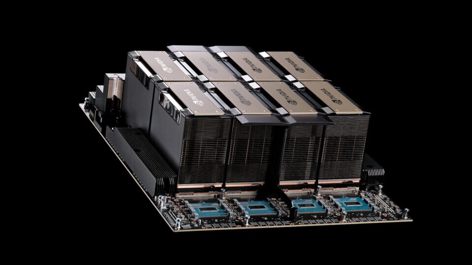
As shown in the figure below, the core of the HGX product is 8 GPUs, which are integrated through the backplane, and also integrate NVLink technology and NVLink SW chips. This “big guy” is designed by NVIDIA, and it is the “smallest form” of the H100 SXM GPU directly provided to the server manufacturer, of course, it cannot work independently, because it is a “logical big GPU”, which must be combined with the server platform (head) to form a complete GPU server.

DGX is an NVIDIA-branded GPU server. As shown in the figure below, in addition to the core HGX module, it is equipped with the chassis, motherboard, power supply, CPU, memory, hard disk, network card and other components that the server should have.
It is not fundamentally different from the GPU servers based on HGX modules that we usually see from major server manufacturers. NVIDIA’s DGX machine is in competition with other server vendors. The first is that the price of DGX is high, and the second is to avoid market conflicts with server manufacturers.

Parameters of Nvidia HGX H100 and H200
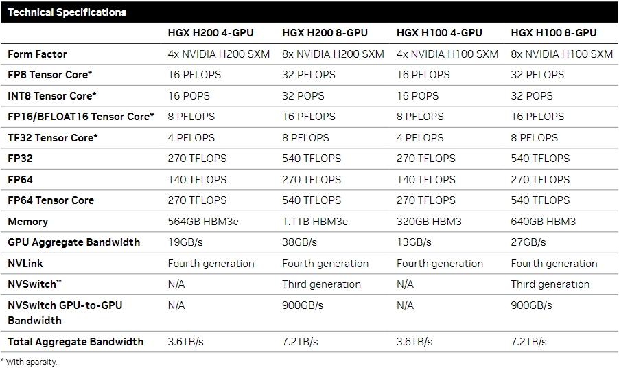
Comparison of HGX H200 and HGX H100
Parameters of DGX H100
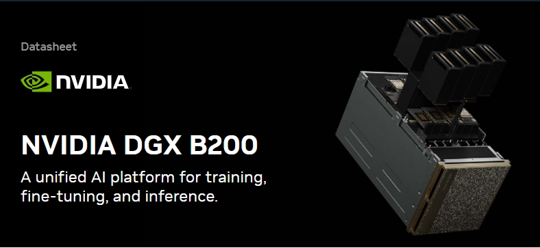
Parameters of DGX B200
Conclusion
NVIDIA HGX and DGX platforms provide flexible solutions for AI and compute tasks of varying scale and demand, from efficient inference on a single GPU to training and inference acceleration at hyperscale data center level.
When purchasing high-speed cable products, it is also crucial to choose a reliable supplier. MVSLINK is a reliable provider of optical network solutions to build a fully connected, intelligent world through innovative computing and networking solutions.


